Unraveling the Complexity of an 8-Layer PCB Stackup: A Comprehensive Guide
Modern technology has led to increasingly complex electronic design landscapes, with diverse applications placing varying demands on electronic components. At the core of many such components lies an indispensable Printed Circuit Board (PCB). As an essential element of modern electronics, PCBs have developed to meet evolving demands ranging from single layer designs up to multi-layer stackups of up to 40 layers. In this article we aim to offer an understanding of an intermediate yet widely utilized form: an 8-layer stackup.
At this first stage of our 8-layer PCB stackup journey, our focus will be conceptual understanding.
Section 1: Introduction to an 8-Layer PCB Stackup
An 8-layer PCB stackup typically comprises eight individual layers of copper-conductive material stacked together with an insulating material such as FR4 epoxy resin insulator between them for electron transport purposes, with additional functions like providing power, signal integrity protection, electromagnetic interference (EMI) reduction and thermal management taking place between each layer.
Section 2: An 8-Layer PCB Stackup’s Roles and Responsibilities
After understanding the concept of an 8-layer PCB stackup, we delve deeper into its functionality. A typical stackup typically comprises signal layers, power plane layers, and ground layers; understanding their role is crucial in understanding its complexity.
Section 3 explores Sequential Build Up (SBU) in depth and its significance within an 8-layer PCB design.
Section 3: The Significance of Sequential Build Up (SBU)
SBU technology plays a pivotal role in PCB manufacturing, particularly multi-layer PCBs. It allows for higher circuitry density while providing additional flexibility to circuit designers who work on 8-layer boards.
As we delve deeper into best practices for designing an 8-layer PCB stackup in Section 4, our knowledge deepens.
Section 4: Strategies for Designing an 8-layer PCB Stackup
Understanding the various layers is only half of the journey to successful PCB design; success comes from applying this knowledge optimally during design phase. Best practices from layer arrangement to via structures can significantly influence an 8-layer PCB stackup’s performance.
Are You Still with us? We hope this intriguing world has kept your interest as it does ours! In the final step of our journey, let’s discuss some prominent applications of 8-layer PCBs.
Section 5: Applications of 8-Layer PCB Stackups
From Aerospace to Medical Electronics, 8-layer PCB stackups find use across numerous industries with demanding requirements. Here we identify some key sectors which significantly rely on 8-layer PCB stackups.
Now we reach the end of our journey; but keep in mind, in technology every new horizon opens up endless opportunities! Stay focused, remain intrigued, and never stop evolving!
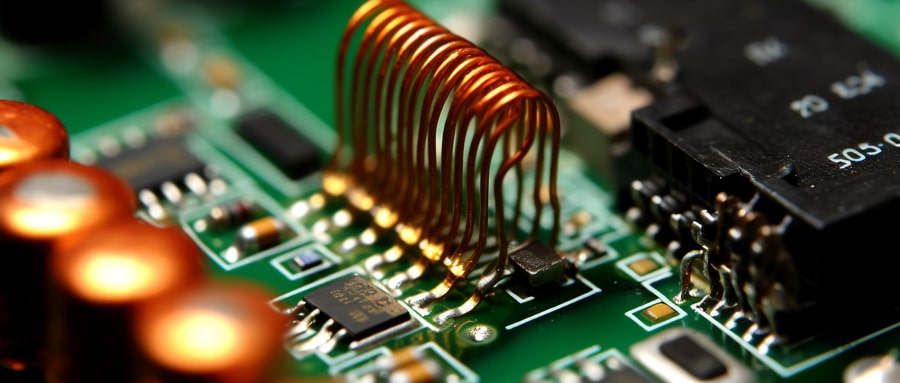
As we have explored the complexity of an 8-layer PCB stackup together, we now appreciate why this seemingly “intermediate” form of PCB can play such an essential role in today and future applications. From signal integrity protection and thermal management to adaptable design matrix capabilities and overall adaptability – these features demonstrate its vital importance among rapid innovation. Its significance fuels our quest to simplify, educate and engage in these explorations further; so until our next electronics-related journey awaits us we bid you goodnight!
[Note: the full version of this article will provide more in-depth coverage of each section, providing greater insights into the complexity of an 8-layer PCB stackup.]FAQ:
- Q: What is an 8 layer PCB?
A: An 8 layer PCB is a printed circuit board that contains eight individual layers of tracks, grounds, and/or signals. - Q: Where are 8 layer PCBs commonly used?
A: They’re often used in complex systems like data servers, GPS technology, and medical systems, where high-speed signals and a compact size are required. - Q: How is an 8 layer PCB constructed?
A: It involves sandwiching eight layers of dielectric material to insulate different layers and traces from each other. - Q: How do the layers of an 8 layer PCB function?
A: Generally, the top and bottom layers are signal layers, and the inner layers serve as power planes, ground, or additional signal planes. - Q: Are 8 layer PCBs for high-speed applications?
A: Yes, 8 layer PCBs are ideal for high-speed applications due to their good signal integrity and reduced electromagnetic interference. - Q: Do 8 layer PCBs perform better than lower layer count PCBs?
A: Yes, due to their complexity, they allow higher circuit density and better electromagnetic interference control. - Q: What are the downsides to using an 8 layer PCB?
A: They are more complex to design and manufacture, and also more expensive due to increased material and labor cost. - Q: What software can I use to design an 8 layer PCB?
A: There are multiple software options, like Altium Designer, OrCAD, and Eagle, that can handle 8 layer PCB designs. - Q: How long does it take to manufacture an 8 layer PCB?
A: The manufacturing time depends on the complexity of the design and the manufacturer, but it’s typically longer than lower layer count PCBs. - Q: What should I consider when ordering an 8 layer PCB?
A: Consider factors like the complexity of your project, cost, your manufacturer’s capabilities, and your project’s lead time.

