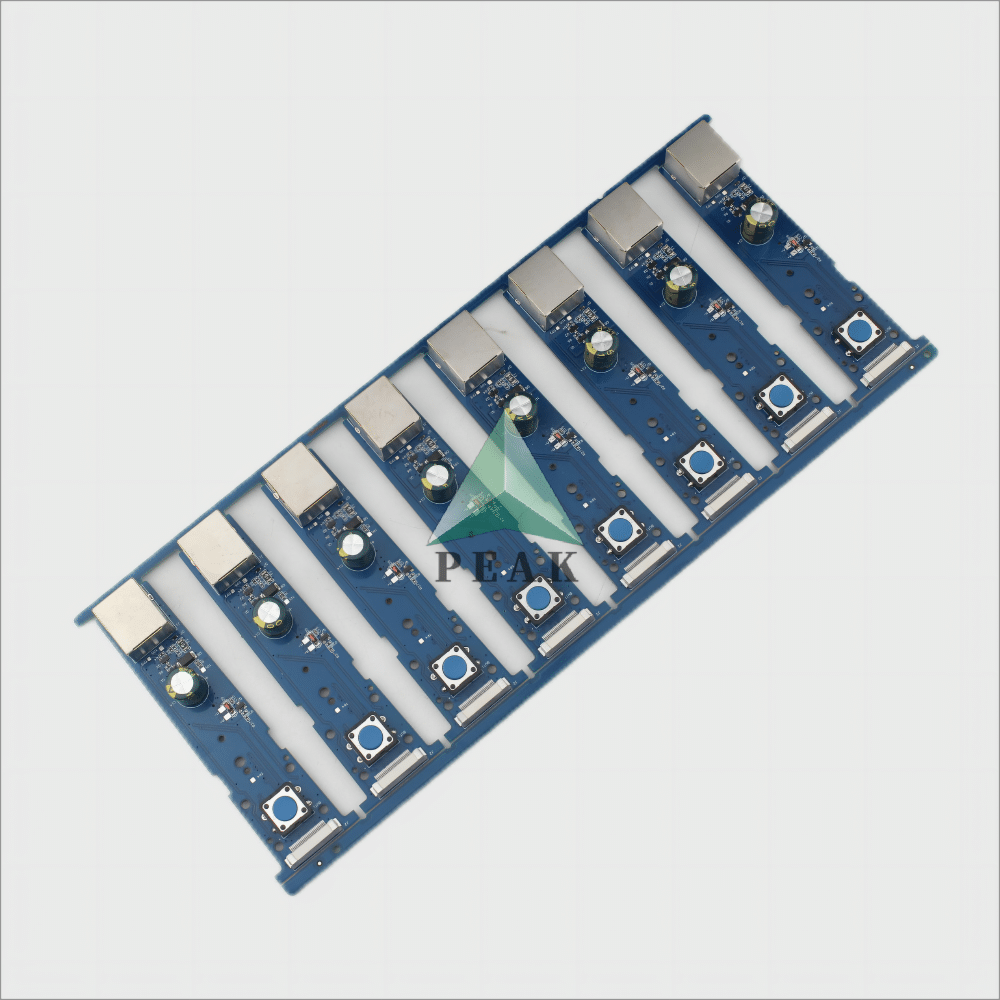
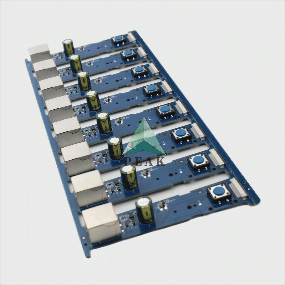
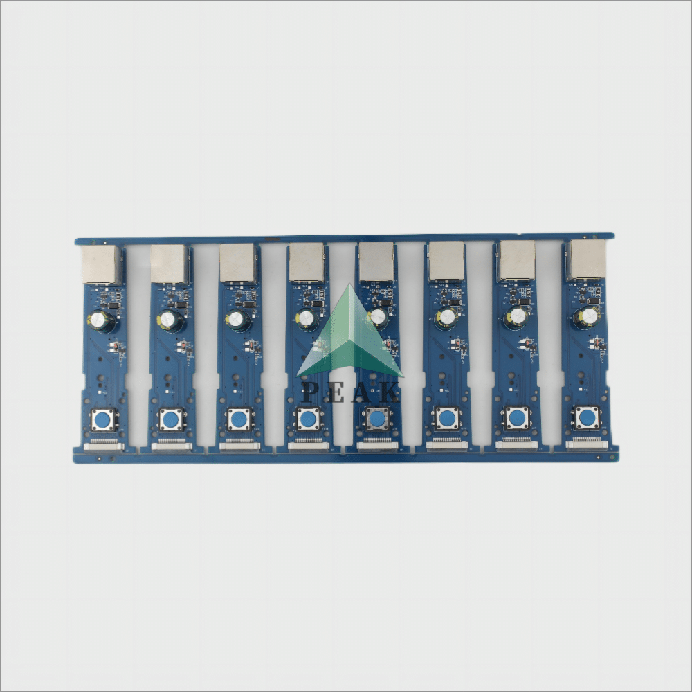
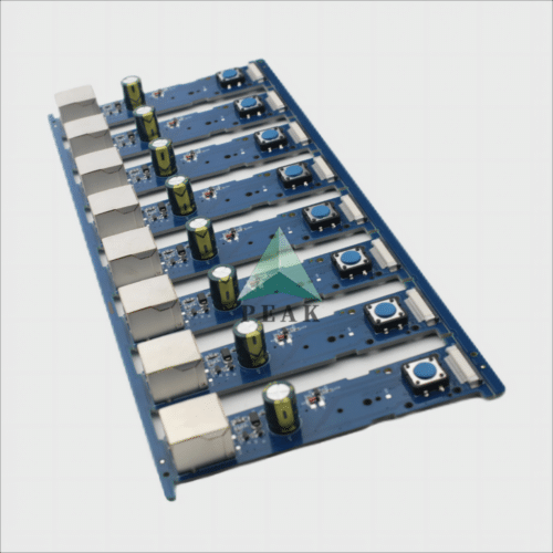
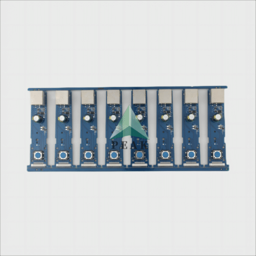
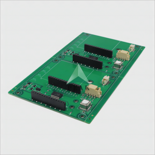
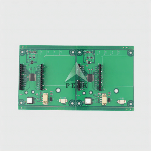
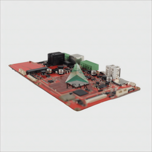
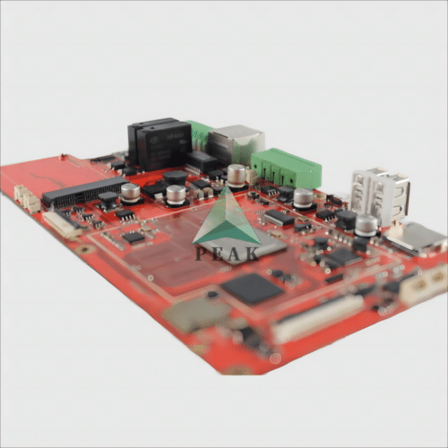
Brand Name : PEAK PCB
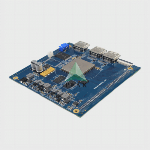
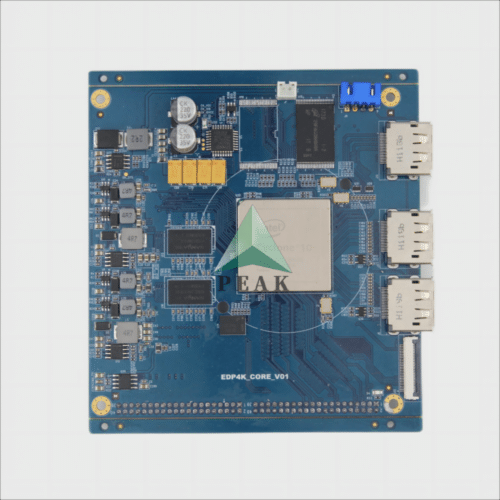
PCB Type : Multilayer PCB
Number of Layers : 4 Layers (Max 64 Layers)
Finished Thickness : 1.6 mm (Max 8mm)
Base Material : FR4 TG170
Finished Inner Copper Thickness : Hoz (Max 14oz)
Finished Outer Copper Thickness : 1oz (Max 14oz)
Min. Mechanical Hole : 0.25 mm (Min 0.1mm)
Min. Line Width : 3.5 mil (Min 2mil)
Min. Line Spacing : 3.5 mil (Min 2mil)
Surface Finishing : ENIG 1u
Solder Mask : Blue
Silk Screen : White
Thickness Tolerance : ±10%
Impedance Control Accuracy : ±10% (min±5%)
Outline Profile : Rout/ V-cut/ Bridge/ Stamp Hole
Testing Service : 100% AOI ICT FCT Testing
Special Processes : No
PCB Standard : IPC-A-610 E Class II
Mounting Component Pitch : 0.15mm
Repeated Accuracy : ±0.01mm
Accuracy of Printing Solder Paste : ±0.025mm
Application : Vehicle Charging Pile
Supply Ability : Sample and Mass Production
Place of Origin : Guangdong, China
Packaging Inner : Vacuum Packing/ Anti-Static Package
Packaging Outer : Export Carton/ Customizable
Port : Shenzhen, Hongkong
Acceptable File Format : Gerber file, Powerpcb, CAD, AUTOCAD, ORCAD, P-CAD, CAM-350, CAM2000
What is PCB Assembly?
PCB assembly, also known as printed circuit board assembly, refers to the process of assembling electronic components onto a printed circuit board (PCB) in order to create a functional electronic device. This process is a crucial step in the manufacturing of electronic devices, as the PCB serves as the backbone for the entire system.
The assembly process begins with the selection of the appropriate PCB based on the specifications of the electronic device being built. The PCB is then populated with electronic components, such as resistors, capacitors, diodes, and integrated circuits, using automated equipment or by hand. These components are secured to the PCB using soldering techniques, including wave soldering or reflow soldering.
Once the components are in place, the PCB assembly undergoes a series of tests to ensure that the electronic device is functioning properly. These tests may include functional testing, in-circuit testing, and visual inspection. Any issues or defects are corrected before the final product is packaged and shipped to the customer.
There are several benefits to using PCB assembly in electronic device manufacturing. PCBs are reliable and durable, and they can be mass-produced efficiently. They also allow for customization, as different components can be added or removed based on the specific needs of the device. PCB assembly also reduces the risk of errors due to human intervention, as automated equipment can accurately place components in the correct locations.
However, PCB assembly does come with some challenges. For instance, the process can be time-consuming and requires specialized equipment and expertise. Additionally, the cost of manufacturing PCBs can be high, especially for small-scale production runs.
Overall, PCB assembly is a critical process in the manufacturing of electronic devices. It allows for the creation of reliable, customizable, and efficient electronic devices that can be mass-produced with minimal errors. While the process does come with its challenges, the benefits of PCB assembly make it an essential component of modern electronics manufacturing.
What is Multilayer PCB?
Multilayer PCB or Printed Circuit Board is a type of board which is used in electronic devices. As the name suggests, it consists of multiple layers of copper conducting paths that are separated by an insulating material called substrate. It is used in high-end electronic devices because of its advantages over the traditional single-layered PCBs.
Multilayer PCBs are made up of multiple layers of conducting paths and insulating materials. These layers are then laminated together to create a single board. The number of layers in a Multilayer PCB can vary depending on the application of the device. Some Multilayer PCBs can have up to 30-40 layers, whereas others may have fewer layers.
The biggest advantage of Multilayer PCBs is their ability to handle complex circuits and designs. Single-layered PCBs have a limited number of components that can be placed on them. However, Multilayer PCBs can accommodate a higher number of components because of their multiple layers. This makes it possible to design more advanced electronic devices.
Multilayer PCBs are also more reliable and durable than single-layered PCBs. The multiple layers provide additional support and stability to the board, making it less prone to damage. The insulating substrate material used in Multilayer PCBs is also more heat-resistant and can withstand higher temperatures without degrading.
Another advantage of Multilayer PCBs is their ability to reduce electromagnetic interference (EMI). The multiple layers of conducting paths in Multilayer PCBs allow for better shielding of the components, reducing EMI. This is particularly important in sensitive electronic devices where EMI can cause interference and disrupt the functioning of the device.
In conclusion, Multilayer PCBs are a superior alternative to traditional single-layered PCBs. They offer the ability to handle complex circuits, are more reliable and durable, and can reduce electromagnetic interference. Multilayer PCBs are widely used in high-end electronic devices such as smartphones, laptops, and other advanced electronic devices.
Have other questions about PCB Assembly?
1. What is PCB assembly?
2. What are the different types of PCB assembly?
3. What materials are used in PCB assembly?
4. How is PCB assembly done?
5. What are the benefits of PCB assembly?
6. What are the challenges in PCB assembly?
7. What is the cost of PCB assembly?
8. What is the turnaround time for PCB assembly?
9. What are the quality standards for PCB assembly?
10. What are the common mistakes made in PCB assembly?

