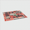
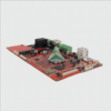
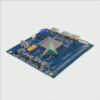
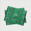
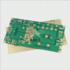
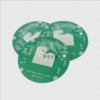
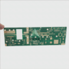
8 layers PCB boards, art in design, you need to know
8 layers PCB board is a kind of multilayer PCB, whose stacked layer structure is realized by combining and designing the materials. When assigning the stacked layer structure, it is necessary to consider factors such as signal quality, power distribution, and grounding protection to ensure the performance and stability of the PCB board.
Generally speaking, the stacking structure of 8 layers PCB boards can be assigned in the following way:
Layer 1: Signal Layer
This layer is the core of the entire PCB and is used to place and connect the main signal lines. These signal lines can be data lines, clock lines, control lines, and so on. In order to ensure the quality of the signals, it is necessary to choose the appropriate line width and line spacing, and to avoid interference between the signals.
Layer 2: Power Layer
This layer is used to distribute power and ground lines to provide stable voltage and current for the entire PCB. In order to reduce power supply noise and signal interference, you can set up a power split grid or use decoupling capacitors to filter.
Layer 3: Ground Layer
This layer is used for ground protection to provide a safe grounding method for the entire PCB board. The ground layout should be as wide as possible to minimize resistance and inductance. At the same time, the ground grid should be kept at a distance from the power supply layer to avoid mutual interference.
Layers 4 to 8: Auxiliary Signal Layers
These layers are mainly used to place other signal lines and components. The appropriate number of layers and layout can be selected according to actual needs. In the auxiliary signal layer, some power or ground layers can also be added as needed to optimize power distribution or strengthen ground protection.
Factors such as the mechanical and thermal properties of the PCB board also need to be considered when assigning the stacked layer structure. For example, it is necessary to select the appropriate material and thickness to ensure the hardness and heat resistance of the PCB board; at the same time, it is necessary to consider the layout of the components and thermal design to avoid problems such as overheating or unstable performance.

