PCB Solder Mask: The Unsung Hero of Circuit Board Production
As one explores the complexity of PCB production, one cannot underestimate the significance of solder mask. Although unseen to casual users but essential to industry professionals alike, solder mask plays an unheralded but integral role in electronics.
This comprehensive article lifts the veil to unveil all the wonders behind PCB solder mask’s varied roles in circuit board production – from shaping its unique aesthetic appearance to guaranteeing its functionality as an electronic device.
Explore PCB Solder Mask Basics
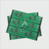
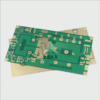
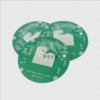
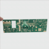
Solder masks for printed circuit boards (PCBs) provide protection from short circuits, solder bridges, and electrical arcing – essential elements in the design and manufacturing processes for electronic devices. However, what makes PCB solder masks such an essential element?
Solder Mask Advantages in PCB Manufacturing
An electronic circuit without solder mask protection can be like a ship without rudder, vulnerable to misdirection and eventual breakdown. Proper solder mask application greatly decreases risk for electronic malfunctions; in this section we explore how solder masks help improve device lifespan, functionality, and reliability.
Types of PCB Solder Masks
Not all solder masks are created equal, each having unique properties and applicable situations. In this section we explore common solder mask types like liquid photoimageable solder mask (LPSM), dry film solder mask (DFSM) and electro-deposition solder mask (EDSM), providing you with the knowledge you need to select an ideal solder mask for any given scenario.
Application Process of PCB Solder Mask
How is solder mask applied onto a PCB and which factors must be considered during application? In this segment, uncover the secrets to successful solder mask application to guarantee high-quality circuit board production.
Common Problems and Pitfalls of Solder Masking
Solder masking, like every manufacturing process, comes with its share of challenges. By understanding common hurdles and taking preventative steps against future incidents affecting quality products, solder masking becomes less risky.
Emerging Trends and Long-Term Perspectives in China’s Economy
Staying abreast of emerging technology trends will set you apart. Gain knowledge about recent industry innovations that may impact or enhance the PCB solder mask application process.
Understanding PCB solder mask can be daunting, but with this comprehensive guidance available to you, you can quickly unravel its complex workings and apply this knowledge in your PCB production process with confidence.
So dive headlong into this PCB solder mask narrative! Learn its types, benefits, application process challenges and future trends before sharpening your skills to navigate an ever-evolving electronics landscape proactively and discover how this unsung hero is shaping electronics history one PCB at a time.
FAQ:
- What is a PCB Solder Mask?
A solder mask, also known as solder resist or solder stop, is a thin layer of polymer used to protect the copper surfaces of a printed circuit board (PCB). Its primary function is to prevent solder bridges from forming between closely spaced solder pads during the soldering process. - What are the advantages of using a PCB Solder Mask?
Aside from preventing solder bridges, a solder mask protects the copper surfaces and traces from oxidation, corrosion, and potential damage from handling. It also enhances the contrast between the board and its traces, improving visual aesthetics and increasing legibility. - In what colours are PCB Solder Masks available?
The most common color for a solder mask is green, but they can also come in other colors such as blue, red, black, white, and yellow. - How is a PCB Solder Mask applied?
The mask is typically applied as a liquid and then hardened by ultraviolet light. Openings in the mask are then made, either mechanically or with lasers, to expose the points on the board where solder is to be applied, such as pads and holes. - Can the PCB Solder Mask thickness be adjusted?
Yes, the thickness of solder mask can be adjusted to some extent. The final thickness often depends on the type of mask material, application method, and curing process, and it will typically range from 0.2mm to 0.4mm. - How does the PCB Solder Mask impact PCB assembly?
The solder mask helps guide the solder to the correct places on the PCB during assembly, reducing the risk of faulty connections. It also prevents the formation of solder bridges and reduces the risk of short circuits. - What material is a PCB Solder Mask made from?
The materials typically used for solder mask include epoxy, liquid photo-imageable solder mask (LPSM), dry film photo-imageable solder mask, and thermal curable solder mask. - How does a PCB Solder Mask affect the longevity of PCBs?
By protecting the copper traces from corrosion, damage, and unwanted solder connections, a solder mask can contribute significantly to the long-term reliability and functionality of a PCB. - Can a PCB be made without a Solder Mask?
While it is possible to make a PCB without a solder mask, it is highly recommended to use one because it provides protection to the copper traces and facilitates precise soldering during PCB assembly. - How do I specify the areas not to be covered by the Solder Mask when designing a PCB?
When designing the PCB, the areas that should not be covered by the solder mask are typically specified in a separate file called the solder mask clearances file, or simply the solder mask file. This includes areas such as component pads and via holes.

