PCB Depaneling: A Comprehensive Guide To Maximizing Production Efficiency
“PCB Depaneling Is Key for Effective Electronics Production”
Depaneling of printed circuit boards (PCBs) has become a vital element of electronics production, helping us produce smaller devices with higher efficiency than ever before. PCB depaneling serves as the cornerstone for success within electronic production environments and should remain such an integral process in future success.
This guide serves as your journey toward understanding and mastering PCB depaneling. Prepare to dive deep into its intricacies, uncover any complexities or realize potential benefits it can bring your business.
PCB Depaneling Definition.
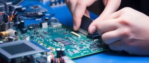
PCB depaneling is the process of breaking or cutting multiple circuit boards manufactured on one panel into individual units for electronics use, in order to lower costs and increase efficiency during production. Depaneling plays an essential part in this journey and should not be skipped over for cost savings or efficiency reasons.
Why Is Depaneling of PCBs Necessary?
Businesses today must continually find ways to increase efficiency, decrease costs and streamline operations in order to remain competitive. PCB depaneling, when done right, can be an economical and practical method of producing bulk units; when done properly it not only speeds up production flow but can even help enhance quality control measures and enhance production outcomes.
Tools and Techniques for Depaneling PCBs
Complex PCB designs vary wildly in complexity, dimensions, and design; thus necessitating different techniques and tools used in their depaneling. This segment explores commonly employed depaneling methods – manual breaking, die cutting, milling routers, laser cutting and V-groove cutting are some of the methods explored here.
How to Select the Appropriate Method for Your Needs
Deciding upon an optimal depaneling technique is no straightforward process, with many factors such as panel size, complexity, material type and production volume being taken into account when making this important decision. This section of our guide offers a thorough analysis of these components so you can make an informed decision for your own operation.
Impact of PCB Depaneling on Design and Prototype Phases
PCB depaneling involves more than the production process alone; design and prototyping decisions have an immense effect on its depaneling process. Our guide describes how proper planning can have an immense impact on production efficiency and cost-effectiveness.
Are You Facing Common Issues and Challenges? Here Are Solutions
Depaneling PCBs presents its own set of challenges. Common areas for concern include risking damage to PCBs, inefficient operations, and handling issues – let’s examine ways we can circumnavigate them to strengthen production journeys and mitigate common obstacles.
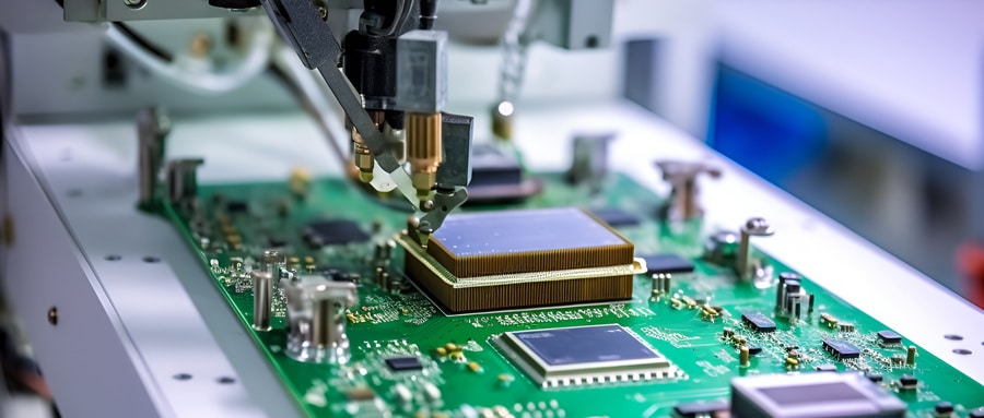
Future of PCB Depaneling
Technology advancement and increasing demands for smaller devices means PCB depaneling continues to evolve rapidly. What lies ahead for PCB depaneling and how can you stay abreast of industry trends? Gain insights into its future success!
By engaging in an in-depth investigation of PCB depaneling, you can increase the efficiency and profitability of electronics production. Your knowledge can help streamline operations, make informed decisions, and craft high-quality products tailored towards market success.
Unleash the power of PCB depaneling today by exploring this insightful guide about its landscape, challenges, solutions, and future prospects.
FAQ:
- What is Printed Circuit Board Depaneling?
Printed Circuit Board depaneling is the process of separating individual PCBs from the panel on which they were initially manufactured. PCBs are typically produced as a panel to maintain consistency and to make handling easier during assembly. Depaneling is usually the final step before the individual boards are shipped. - What are the different methods of Printed Circuit Board Depaneling?
There are several methods of Printed Circuit Board depaneling including manual breaking, die cutting, milling cutters, laser cutting, and using a depaneling router. - How is manual breaking done in Printed Circuit Board Depaneling?
Manual breaking, or hand-breaking, is the simplest form of depaneling where panels are manually broken along perforated lines. This method is less common now due to increased requirements for precision. - What is the most common method for Printed Circuit Board Depaneling?
The utilization of depaneling routers has become prevalent in Printed Circuit Board depaneling due to their high precision, flexibility, and capabilities for stress reduction. - What is the purpose of Printed Circuit Board Depaneling?
Depaneling is primarily done to convert the large panel into individual boards for use in end products. It also makes the handling, testing and packaging of the PCBs easier. - Is Printed Circuit Board Depaneling done before or after assembly?
Depaneling is generally performed after the components have been soldered onto the PCB panel during assembly. However, the exact point in the process can vary based on a variety of factors, including the type of components used and the specifics of the production line. - What kind of care needs to be taken during Printed Circuit Board Depaneling?
During depaneling, it’s vital to maintain minimal stress on the PCB to limit potential damage. This is particularly important for PCBs with close component layout or delicate parts. - Does the size of the PCB affect the Depaneling method?
Yes, the dimensions of the PCBs can significantly affect the choice of depaneling method. For example, larger PCBs might not fit into certain machines and may require more manual or elaborate methods. - What are some challenges in Printed Circuit Board Depaneling?
Some challenges in Printed Circuit Board depaneling include potential damage to the board or components, ensuring clean edges, managing dust and scraps from the depaneling process, and maintaining a fast and precise operation. - Are there any recent advancements in Printed Circuit Board Depaneling?
Advancements such as laser cutting machines have made the process of Printed Circuit Board depaneling more precise and less stressful on the PCB. These machines use a directed laser to cut the PCB along the required lines, minimizing physical contact and potential damage.

