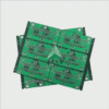
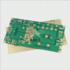
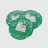
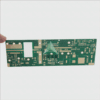
Multi Layer PCB: Deep Dive into Applications and Manufacturing Process
Technology’s rapid advances across many sectors has driven unprecedented change across our world, but none more so than with respect to Printed Circuit Boards (PCBs). PCBs serve as the cornerstone of electronic devices, orchestrating various functionalities seamlessly and reliably. This article seeks to examine one particular form of PCB – Multi-Layer Printed Boards – their numerous applications, and manufacturing process in depth.
Multi Layer PCBs: What Exactly Do They Consist of?
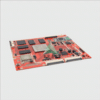
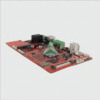
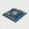
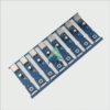
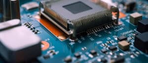
Multi-layer PCBs (or multilayer circuit boards, PCBs for short) are made up of multiple two-layer PCBs bonded together into one seamless compound structure. As opposed to single or double layer PCBs which only contain circuitry on one or both sides, multi-layer PCBs may contain as many as dozens of separate layers built up in one piece – an advantage many electronic devices rely on due to their high capacity, durability, and compact nature.
Layers of Utility: Applications of Multi Layer PCBs
Multi-layer PCBs form the heart of many of the devices we rely on daily, including high-speed computers, communication systems, GPS technology, heart monitors and even military technology. Their versatility stems from their high density assembly capability and stability under changing temperatures compared to single or double layer boards; further demonstrating their worth as an invaluable resource.
Beginning of Production Process of Multi Layer PCB
Manufacturing multi-layer PCBs involves multiple carefully calibrated steps. Starting from inner layer photoprint to outer layer imaging, every phase must be closely monitored for successful execution. Notable steps of this process include inner layer etching, layer alignment, bonding drilling plating plating solder mask application solder mask application solder mask removal final finishing. Multi-layer PCBs offer exceptional performance and efficiency design features which require this intricate manufacturing process to produce quality designs that meet those standards.
Conclusion: Multi Layer PCBs Are The Future
As technology demands smarter and smaller devices with advanced features, multi-layer PCBs have grown increasingly important. Not only is understanding their engineering vital for industry stakeholders but it’s also essential for everyday tech enthusiasts who rely on devices.
This comprehensive guide has provided an in-depth exploration of multi-layer PCBs, their wide array of uses, and their complex production process. Hopefully it has shed some light on this important technological component for those unfamiliar with it; multi-layer PCBs’ influence and presence is only set to grow.
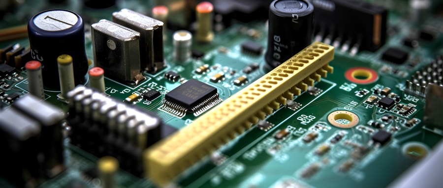
As we advance further in our scientific era, exploring and understanding intricate components like multi-layer PCBs is increasingly crucial to further advancements. Not only can this knowledge lead to improved innovations, but it can also illuminate what goes behind our daily gadgets – becoming informed users. Let’s discover more of technology step by step! Let’s continue advancing into it together.
FAQ:
- What is a Multi Layer PCB?
A Multi Layer PCB refers to a printed circuit board that features more than two conductive copper layers. These conductors are embedded in the insulation of the board and connect to the circuits on different layers with vias. - What are the benefits of Multi Layer PCBs?
Multi Layer PCBs offer numerous benefits such as higher assembly density, easier incorporation of more advanced features, better noise reduction and higher circuit speed. They are also lighter and smaller, making them ideal for today’s increasingly compact and complex electronic devices. - How many layers do Multi Layer PCBs usually have?
There’s wide variation in the number of layers that a multi-layer PCB can have, but some common configurations include 4, 6, 8, or 10 layers. However, for very complex circuitry, PCBs with over 40 layers can be fabricated. - Are Multi Layer PCBs more expensive to produce?
Yes, multi-layer PCBs are generally more expensive to create than their single or double-sided counterparts. This is due to the additional materials and more complex manufacturing process required. - 5. What are the common applications of Multi Layer PCBs?
Multi Layer PCBs are used in various industries such as telecommunications, medical electronics, military and aerospace application, consumer electronics, and computer systems where high-density and complex circuitry are required. - How are the layers in a Multi Layer PCB connected?
The layers in a Multi Layer PCB are interconnected via drilled holes known as vias. These vias pass through the layers and are then plated with copper to provide the electrical connections. - How is the design and layout of Multi Layer PCBs done?
The design and layout of multi-layer PCBs use special PCB design software. The process can be intricate and complex due to the necessity to route multiple layers while maintaining signal integrity and adhering to design rules. - Are Multi Layer PCBs more durable?
Multi Layer PCBs tend to be more robust and can endure higher levels of stress. They are designed to handle higher speeds and more intensive applications. - How does Multi Layer PCB fabrication process work?
The multilayer PCB fabrication process involves several steps including layer stack up, copper foil lamination, drilling, plating, imaging and etching, and finally, testing. - Does the use of Multi Layer reduce electromagnetic interference (EMI)?
Yes, one of the advantages of a multi-layer PCB is the reduction of EMI. By placing critical layers between ground and power plane layers, both shielded and noise-immunity can be achieved.

