Network PCB Design: Building Reliable and Efficient Network Systems
Network PCB Design: Building Reliable and Efficient Network Solutions
Network systems are at the core of modern communications. Reliable and efficient network PCB design plays an integral part in ensuring their smooth functioning and performance, from signal integrity through power delivery, thermal management, to compliance with EMI/EMC requirements. In this article, we’ll outline key considerations and best practices when designing network PCBs – with focus on signal integrity, power delivery, thermal management, thermal management compliance requirements as well as EMI/EMC regulations.
Signal Integrity:
Maintaining signal integrity in network PCB design is of utmost importance in order to guarantee reliable data transmission and reduce errors and signal degradation risks. Designers must take careful note when considering trace routing, impedance control, ground and power plane allocation as well as reflections, crosstalk, signal integrity issues as a whole – using design tools with advanced simulation and analysis capabilities will guarantee optimal signal performance.
Power Delivery:
Efficient power delivery is crucial for network components’ successful functioning and ensuring stable operation, so designers must carefully plan power distribution networks (PDNs). By employing proper trace widths, power plane designs, decoupling capacitors and voltage regulators in PDN designs, voltage drops, noise and power supply fluctuations can be reduced significantly while still guaranteeing reliable and consistent power distribution to network devices.
Thermal Management:
Network systems generate heat, and effective thermal management is vital to ensure their reliability and lifespan. Designers should take note of proper component placement, heatsinks, thermal vias and adequate airflow in order to dissipate heat effectively. Thermal analysis tools can identify hotspots while optimizing performance to keep components within safe temperature limits.
EMI/EMC Compliance:
Electromagnetic interference (EMI) and electromagnetic compatibility (EMC) issues can seriously impede network performance. Designers must incorporate EMI/EMC mitigation techniques from the initial design stage onward. These may include carefully routing high-speed traces, using suitable grounding techniques, shielding components properly, filtering components, and shielding the network components accordingly. Compliance with EMI/EMC regulations helps prevent signal interference for optimal network performance in various environments.
Considerations in High-Speed Design:
Network PCBs typically contain high-speed signals like Ethernet, USB, or PCIe that require designers to take careful consideration in routing controlled impedance routing, differential pair routing, matched trace lengths, signal integrity analysis, timing skew minimization analysis tools as well as signal integrity simulation tools to maintain signal integrity for reliable data transmission.
Component Selection and Footprint Planning:
Selecting components for network PCBs is essential for optimal system reliability and performance, so designers must carefully consider compatibility, reliability, power consumption, availability and footprint design features that ensure accurate component placement, optimal soldering practices and efficient manufacturing processes.
Prototyping and Testing:
Testing is essential in network PCB design to validate and ensure its performance, from functional tests, signal integrity analysis, performance benchmarking and iterative prototyping cycles that lead to optimized designs that ensure reliable network systems.
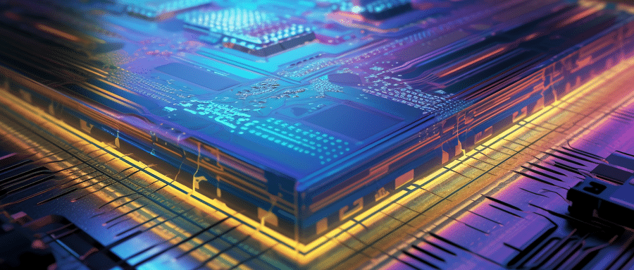
Designing reliable and efficient network PCBs with signal integrity, power delivery, thermal management and EMI/EMC compliance as their top priorities is essential to creating reliable network systems. Following best practices and making use of advanced design tools and simulation software to design network PCBs that meet these criteria helps designers ensure network PCBs that meet data transmission needs at high speeds while offering stable power delivery, mitigating thermal issues and adhering to EMI/EMC regulations – ultimately helping achieve seamless communications and connectivity in digital spaces.
FAQ:
- What is a Network PCB?
A Network PCB refers to a Printed Circuit Board used in a network device, such as a router, modem, switch, or other devices used in telecommunications, data communications, and wireless communications. - How do Network Printed Circuit Boards function?
Network Printed Circuit Boards house the integrated circuits, resistors, capacitors, and other components that control the operation of the network device. The hardware design, controlled by the device’s firmware, helps regulate the flow of data across networks. - What are the elements of a Network Printed Circuit Board?
A Network Printed Circuit Board typically includes components like microcontrollers, capacitors, Integrated Circuits (ICs), resistors, connectors, and light-emitting diodes (LEDs). The arrangement of these components can vary based on the type of network device. - How are Network Printed Circuit Boards designed?
Network Printed Circuit Boards are designed using PCB design software, with careful consideration to EMI (Electromagnetic Interference), signal integrity, power distribution, thermal heat dissipation, and FCC compliance for wireless devices. - What challenges does Network Printed Circuit Board design present?
Network Printed Circuit Boards often have high-frequency signals that can present challenges with EMI and signal integrity. These boards may also require special materials for managing heat dissipation or high-frequency performance. - Are Network Printed Circuit Boards different than normal PCBs?
While the fundamental conductive and insulating properties remain the same, Network Printed Circuit Boards might require more layers and may be designed for higher frequencies to cater to networking bandwidth requirements. - Why is careful component placement critical in Network Printed Circuit Boards?
In Network Printed Circuit Boards, where high-frequency signals are continually transmitted, careful component placement is critical to reduce signal interference, optimize data transfer paths, and ensure effective heat dissipation. - How has the growth of IoT impacted Network Printed Circuit Board design?
With IoT, circuits need to be small, powerful, and energy-efficient. This calls for PCBs that can support wireless communications, low power consumption, and miniaturization. - What kind of tests are carried out on Network PCBs?
Network PCBs go through various tests to ensure quality and functionality, like continuity tests, insulation resistance tests, environmental tests, and FCC certification tests for wireless devices. - Can Network PCBs support multiple networking standards?
Yes, Network PCBs can support multiple networking standards like Ethernet, Wi-Fi, Bluetooth, GSM, LTE, depending on the specific requirements and capabilities of the networking device in which it is used.

