Impedance Control PCB Design: Enhancing Signal Integrity and Performance
Understanding and controlling impedance are central components of high-speed PCB (Printed Circuit Board) design, as they ensure signal integrity. This article seeks to demystify these concepts, methodologies, and significance for PCB design with the goal of helping create high-performing electronic circuits.
Unveiling Impedance Control Systems
Impedance, which combines resistance and reactance, determines how a circuit resists flow of an AC signal. PCB design offers Impedance Control as a process that ensures consistent impedance across traces in order to guarantee accurate signal transmission without distortion or loss.
An Impression on Impedance Management
As electronic systems continue to miniaturize while also increasing signal speeds, the risk of signal distortion or electromagnetic interference (EMI) increases. Impedance mismatches may cause signal reflection that disrupts data transmission; an effective impedance control strategy must be employed in high-frequency/high-speed applications where maintaining signal integrity is of critical importance.
Methods of Impedance Control PCB Design
Here are a few key techniques for minimizing impedance PCB design:
- Correct Trace Dimensioning: Traces play a critical role in PCB impedance, so accurate calculation and consistent geometry across the design are essential.
- Consideration of Dielectric Material: Dielectric materials can have an enormous effect on board impedance; their thickness has to be taken into account during calculations of impedance. Their dielectric constant should also be considered.
- Careful Routing Practices: For high-speed signals, optimal impedance stability requires routing traces over an uninterrupted reference plane. Any breaks may result in discontinuities that compromise signal integrity.
- Achieve Balanced Capacitance and Inductance: To achieve a particular impedance, capacitive and inductive reactances must be evenly balanced throughout a PCB design, in order to maintain its specific impedance value. Failure to do so could significantly compromise its signal transmitting capabilities and performance overall.
- Utilizing PCB Design Tools: EDA (Electronic Design Automation) tools provide impedance calculators that assist designers with selecting the appropriate trace geometry to meet desired impedance levels.
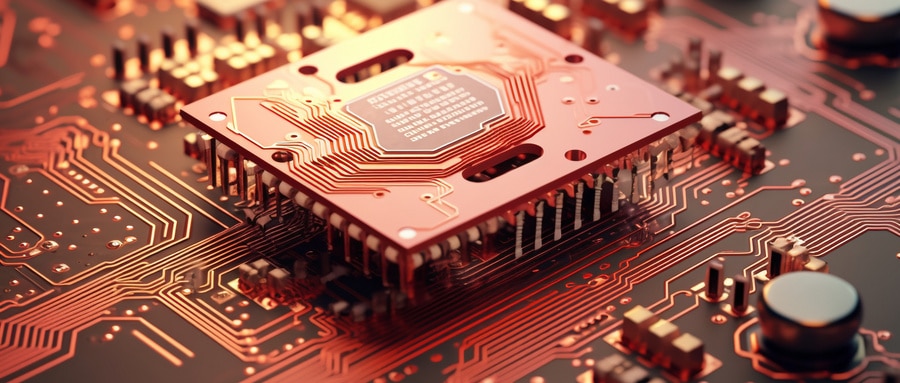
Impedance control is integral in maintaining signal integrity on high-speed PCB designs. By understanding key factors affecting impedance and employing effective strategies to manage impedance issues, designers can manage impedance challenges effectively and ensure development of high-performing electronic solutions with superior reliability.
FAQ:
- Q: What is Impedance Control PCB?
A: Impedance control PCB is a practice to design the PCB to have a specific impedance, calculated using parameters such as trace width, trace thickness, substrate height, and dielectric constant. - Q: Why is Impedance Control important in PCB design?
A: It’s crucial for preserving signal integrity in high-frequency or high-speed digital circuits. Controlled impedance prevents signal distortion, cross-talk, and signal reflection at the termination. - Q: How is controlled impedance achieved in PCB design?
A: It’s achieved by appropriate design configurations in the PCB layout, such as specific trace widths, dielectric thicknesses and constant, and careful consideration of distances between layers. - Q: Can any PCB have Impedance Control?
A: Yes, but it is especially critical for high-speed or high-frequency applications where signal integrity is paramount. - Q: What factors influence the impedance of a PCB?
A: Several factors, including trace thickness, width, and materials; the properties of the dielectric material between the layers; the distance between the trace and the reference plane, etc. - Q: Can a manufacturer check the impedance of a PCB after it’s made?
A: Yes, PCB manufacturers use a TDR (Time-Domain Reflectometer) to test and confirm the PCB’s impedance after it’s manufactured. - Q: Does Impedance Control add to the cost of the PCB manufacturing?
A: Yes, impedance control usually increases the cost of PCB production due to the need for careful calculations, more precise manufacturing processes, and extra testing. - Q: What applications typically require Impedance Control PCB?
A: High-speed digital applications (like RF communication and fast data rate systems), telecommunication systems and network systems often require Impedance Controlled PCBs. - Q: What happens if the impedance isn’t controlled or is off-target?
A: Uncontrolled or mismatched impedance can lead to signal reflections, causing signal integrity issues, which can disrupt the performance of the PCB and the overall device. - Q: Can the impedance of a PCB change over time?
A: Normally, the impedance of a PCB should remain fairly constant, provided the PCB is not subjected to conditions that significantly alter its material or structural properties.

