PCB Panels: Insights into Design, Function, and Optimization Techniques
PCBs power most modern electronics devices, whether single boards or assembled as panels. Electronic manufacturing services (EMS), however, have increasingly used PCB panels as an innovation to maximize efficiency while streamlining operations and cutting costs. This article delves deep into PCB Panels by outlining their design features, functions, and tips on optimizing their usage.
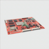
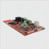
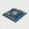
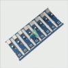
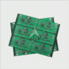
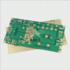
PCB Panels, commonly referred to as arrays, are large circuit boards made up of several smaller boards (known as modules), designed specifically to make assembly of many boards at once simpler and more efficient – an essential aspect for automating assembly processes.
Design of PCB panels may appear complex, yet specific guidelines exist to maximize efficiency in their construction. First and foremost, each individual board making up the panel should be laid out to utilize maximum space while still preserving structural integrity; these gaps are known as breakaway rail or tab route and help separate units after assembly; it should also be precisely calculated so as not to prevent movement while arrayed.
Separating panels into individual modules typically involves two techniques – Break routing and V-scoring. Break routing involves adding perforations or breakout tabs to make separation of boards post assembly simpler; V-scoring involves scoring lines halfway into both top and bottom surfaces of boards that allow them to be easily disassembled later on.
Optimizing PCB panels takes knowledge and expertise. Some tips for optimization of these panels include:
- Maintain a uniform shape and size across all modules to facilitate effortless assembly, which will decrease assembly times.
- Leave enough space between modules in order to minimize any possibility of them breaking during assembly or transport.
- Place fiducial markers at each board corner and on panels for easier assembly. This will aid in alignment during assembly.
By optimizing PCB production using panels, industries have found ways to streamline electronic device manufacturing while increasing product quality.
Understanding PCB Panels – their design, functionality and optimization – is of great value for anyone involved in electronics industry. As PCB panels become ever more prevalent in assemblies, having an in-depth knowledge will only enhance efficiency and quality during assembly processes.
This comprehensive guide offers insight into the complex world of PCB Panels for students, professionals, and anyone with an interest in electronics.
PCB Panel FAQ:
- What is a PCB Panel?
A PCB Panel refers to a group of Printed Circuit Boards which are fabricated on a larger board, also known as a panel. The idea behind this is to make the handling of the PCBs easier during the manufacturing process, especially for automated assembly processes. - Why use a PCB Panel instead of separate boards?
PCB Panelization can improve the throughput and efficiency of the PCB assembly process. It helps reduce the set-up time for each board, allows simultaneous assembly of multiple boards, and reduces the risk of damage to individual PCBs. - How does the panelization process work?
Panelization process includes the arrangement of smaller PCBs onto a larger panel by methods like V-score or Tab-route. This larger panel eases the conveying, solder paste printing, component mounting and reflow processes. - Can I choose my own Panel size?
Yes, you can, but it often depends on the requirements of the PCB manufacturer. They will generally have certain guidelines or restrictions to ensure efficient production. - What is V-Score panelization?
V-Score panelization is a method where a V-shaped groove is cut on both the top and bottom sides of the panel, leaving a thin layer in the middle. This allows the boards to be easily broken apart after the assembly process. - What is Tab-route panelization?
In tab-route panelization, small tabs are used to connect each PCB to the panel frame. After the assembly is complete, these tabs are either cut or broken off to separate each board. - How can I decide which Panelization method to choose?
The choice between V-Score and Tab-Route often depends on the design of the PCB, the requirements of the assembly process, and the tolerances needed for your specific application. - What is the cost of Panelization?
The cost of panelization can vary depending on the complexity of the PCBs, the panelization method, and the manufacturer. It’s best to check with your chosen PCB manufacturer. - Can any PCB design be panelized?
While most PCB designs can be panelized, certain designs might not be ideal due to their dimensions, complexity, or specific requirements. - What are the potential challenges with PCB Panelization?
Potential challenges can include breaking of the boards when depanelizing, design errors being multiplied across the panel and increased material waste. To avoid these issues, it’s important to work closely with your PCB manufacturer during the design and production process.

