PCB Antenna Design: A Crucial Element of Next-Generation Wireless Communication
Wireless technologies have seen remarkable advancements recently. One key facet often neglected in this technological revolution is Printed Circuit Board (PCB) antennas; an integral part that holds great sway over wireless communication. In this article we aim to educate readers on these fascinating antennas with regards to design process, efficacy, and potential future uses.
1. The Genesis
PCB Antennas At first glance, PCB antennas may seem to have emerged alongside wireless technology’s advent; but that is only partly true. Their history goes back to late 19th century pioneers like Nikola Tesla and Guglielmo Marconi making strides into wireless communication; relatively simple designs during those times evolved over time into efficient yet low-cost PCB antennas that form key components of modern wireless systems.
2. What Is A PCB Antenna?
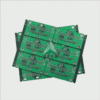
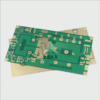
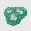
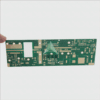
PCB antennas, more commonly referred to as trace antennas, are antennas built into circuit boards to facilitate wireless communication. They typically consist of copper tracks etched onto the board as antenna traces – giving rise to another moniker for them: “etched antennas”. PCB antennas play a pivotal role in many devices including WiFi routers, mobile phones and GPS units.
3. Design of PCB Antennas
The design of PCB antennas requires careful thought. In particular, consideration must be given to its actual environment in terms of PCB material thickness, size and surrounding electronic components – these factors all play a part in its performance. Substrate materials have an immense effect on this aspect.
4. The Efficacy
PCB antennas have gained in popularity thanks to their efficiency, compact size and cost-effectiveness. An antenna’s performance depends on several parameters such as gain, radiation pattern and polarization – PCB antennas excel in each of these categories and moreover allow customization to meet a wide variety of applications further increasing their appeal.
5. Our Vision for the Future – A Roadmap
PCB antennas look set for a promising future. As wireless technology continues to advance, demand for efficient yet compact antennas will only continue to increase. 5G technology and the Internet-of-Things (IoT) promises to further drive interest in PCB antennas; innovations that increase integration, miniaturization, multifrequency support will surely follow soon after their debut.
Designing a PCB antenna requires both creativity and technical know-how, and as we transition into an age of wireless connectivity it becomes essential to recognize this key player’s role and application spectrum. A PCB antenna with its individual characteristics and profound impacts has earned its place as an integral element of wireless communications.

This article presents an in-depth understanding of PCB antennas and their role in modern wireless communication. From their beginning, intricacies of design, efficacy and possible future plans – placing it at the epicenter of wireless revolution. As we move further into the future it seems clear that their significance is only increasing; today it’s not just an option – it’s essential!
FAQ:
- Q: What is a Printed Circuit Board (PCB) antenna?
A: A Printed Circuit Board antenna is a type of antenna which consists of a trace drawn on a PCB. This can provide a compact and efficient antenna design, especially for RF and microwave applications. - Q: What are some common types of Printed Circuit Board antennas?
A: Different types include monopole, dipole, patch, and loop antennas. They can be utilized depending upon the application and frequency range. - Q: What are the benefits of using a Printed Circuit Board antenna?
A: Printed Circuit Board antennas can be compact, cost-effective, and efficient. They can also be easily mass-produced, integrated with electronics on the same PCB, making them ideal for many applications. - Q: What factors need to be considered when designing a Printed Circuit Board antenna?
A: The size and shape of the board, the frequency of operation, the required gain, directivity, and impedance matching are among the main factors. - Q: How do I match the impedance of a Printed Circuit Board antenna?
A: This can be achieved by using different matching networks, like LC (inductor-capacitor) networks. The specific matching network depends on the application and antenna type. - Q: Can Printed Circuit Board antennas be used for MIMO (Multiple Input Multiple Output) systems?
A: Yes, multiple Printed Circuit Board antennas can be placed on a single board to create a MIMO system which can improve performance and increase wireless capacity. - Q: What is the role of the ground plane in a Printed Circuit Board antenna?
A: The ground plane can help reflect the signal and thereby increases the antenna gain. It should be kept free from components and traces to avoid interference. - Q: How can Printed Circuit Board antennas be tested?
A: They can be tested in an anechoic chamber for radiation pattern, return loss and gain, among other parameters. - Q: Can Printed Circuit Board antennas be used for IoT devices?
A: Absolutely, Printed Circuit Board antennas are widely used in IoT devices due to their compact size and cost-effectiveness. They can readily interface with wireless chips and modules. - Q: What can cause a Printed Circuit Board antenna to perform poorly?
A: Factors such as improper impedance matching, incorrect size or trace design, and interference from other components can negatively affect the performance of a Printed Circuit Board antenna.

