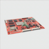
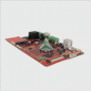
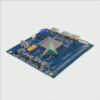
Exploring the World of Donut Hole PCBs – Innovative Solutions for Electronics
Today’s fast-paced world makes electronics an indispensable part of life, from our smartphones and household appliances to printed circuit boards (PCBs) powering these devices and providing their foundation – one innovative type gaining increasing attention is donut hole PCB.
What Are Donut Hole PCBs?
Donut hole PCBs, as their name implies, are printed circuit boards featuring one or more holes or cutouts in their centers that feature copper plating to connect different layers on the PCB. Compared to traditional through-hole vias, donut hole vias provide a unique approach for interconnection and space optimization that stands out.
Donut Hole PCBs Have Many Features and Advantages:
- Improved Space Utilization: Donut hole PCBs enable more effective use of PCB real estate by eliminating separate drilling for each via, providing greater use of its center area by designers looking for additional components to add, reduce size or accommodate complex circuit designs in space-constrained applications.
- Increased Signal Integrity: Donut hole PCB designs eliminate parasitic capacitance and inductance associated with traditional vias, providing enhanced signal integrity with reduced signal loss and superior high-frequency performance, making these boards ideal for high speed designs and applications.
- Thermal Management: Donut hole PCBs feature hollow centers to facilitate efficient heat dissipation, making them suitable for applications that demand effective thermal management. Their thermal vias help move away from components that generate excess heat, guaranteeing optimal performance and reliability.
- Increased Design Flexibility: Donut hole PCBs allow designers more freedom in terms of routing traces and placing components, thanks to their lack of traditional through-hole vias that typically restrict routing options. This increased design flexibility contributes to greater design efficiency as well as better performance for a given design project.
Applications of Donut Hole PCBs:
- Consumer Electronics: Donut hole PCBs find wide application in consumer electronics devices such as smartphones, tablets, wearables and gaming systems. Their compact size, improved signal integrity and thermal management capabilities make them an excellent solution for space-constrained and high-performance devices.
- Automotive Industry: The automotive industry requires reliable electronic systems. Donut hole PCBs are becoming more prevalent in cars due to their ability to withstand harsh environments, efficient thermal management, and space-saving benefits – they’re commonly found in electronic control units (ECUs), infotainment systems and advanced driver assistance systems (ADASs).
- Aerospace and Defense: PCBs designed specifically for aerospace and defense use must withstand harsh environments while meeting stringent performance criteria. Donut hole PCBs excel in these regards, offering improved reliability, improved signal integrity, and effective thermal management to meet these stringent demands – they play a pivotal role in avionics systems, communication equipment, and military radar systems.
- Medical Devices: Donut hole PCBs have become an invaluable addition to medical devices that require precision and reliability, including implantable devices, diagnostic equipment, and monitoring systems. With their compact size, improved signal integrity capabilities, thermal management capacities, and thermal management features donut hole PCBs are becoming an excellent way to manage thermal stressors in this sector.
Donut hole PCBs represent an enormous advancement in electronics. Their distinctive features, including enhanced space utilization, improved signal integrity, effective thermal management and increased design flexibility make them an excellent solution for a range of applications. As technology continues to advance, donut hole PCBs may play a pivotal role in shaping its future – helping create smaller devices with higher performance than before! Seize this innovative opportunity today and unlock an abundance of possibilities in electronics!
FAQ:
- What is a Donut Hole PCB?
The term “donut hole PCB” is not a standard term in the PCB manufacturing industry. You may be referencing via holes (sometimes colloquially referred to as ‘donut holes’) which are holes drilled into a PCB to create electrical connections between the layers of the board. - What are Via Holes in PCBs?
Vias are small holes in a PCB that are filled or plated with metal. They serve to connect different layers of a multilayer PCB, allowing signals to pass through from one layer to another. - What are the Different Types of Vias?
There are three types of vias used in PCB design: Through-hole Vias, Blind Vias, and Buried Vias. Through-hole vias pass completely through the PCB, blind vias connect an outer layer to one or more inner layers but do not go through the entire board. A buried via connects two or more inner layers and does not reach the outer layers. - How are Vias formed in a PCB?
Before the PCB is assembled, holes are drilled at the designated points according to the design specifications. These holes are then plated with an electrically conductive material like copper to create a connection between the layers. - What are the Functions of Vias?
Vias are used to route signals from one layer to another, to provide grounding paths, and to help dissipate heat from components. - What is Via-in-Pad?
Via-in-pad is a design technique in which a via is placed directly beneath the component pad. This is often used for high-speed designs or components with a large number of pins, such as BGAs. - What are Micro Vias?
Micro vias are small vias (usually less than 0.15 mm in diameter) used in high-density interconnect (HDI) boards. They can be used for fine-pitch BGA devices or for routing in very dense areas. - How is the Size of a Via Determined?
The size of a via is determined by several factors, including the current it needs to carry, the space available on the PCB, and the capabilities of the PCB manufacturer. - Can Vias Affect the Performance of a PCB?
Yes, the design and placement of vias can affect the performance of the PCB, especially in high-speed or high-frequency circuits. Vias can introduce parasitic capacitance and inductance into the circuit, affecting signal integrity. - What is Via Filling?
Via filling is a process where vias are filled with non-conductive or conductive materials to prevent solder from wicking away during reflow, to provide structural support, or to allow for a flat surface for component placement.

