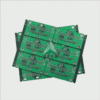
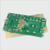
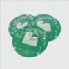
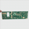
Unveiling the Magic of Silkscreen PCB Design: A Comprehensive Insight
Silkscreening is an essential element of printed circuit board (PCB) design that’s often neglected in favor of more intricate elements. It provides critical information that assists with assembly, testing, servicing and troubleshooting operations – something this guide explores further in depth.
1. What are Silkscreen PCBs?
Silkscreening refers to the layer of ink traces used to identify components, test points, parts of a PCB assembly and any pertinent details about board assembly. Silkscreen is an essential element of PCB production that assists stakeholders at various stages from assembly through repair.
2. Varieties of Silkscreen Processes:
Silkscreen printing on PCBs typically involves three methods of silkscreening: manual screen-printing, Liquid Photo Imaging (LPI), and Direct Legend Printing (DLP). While manual screen-printing remains economical and time-tested, LPI and DLP provide increased precision and resolution.
3. Design Considerations for Silkscreen Printing:
Designing the silkscreen for a PCB requires consideration of several key factors, including text clarity, size, orientation and placement. It’s essential that all information presented on the silkscreen be legible and not interfere with soldering pads, holes or component placement.
4. Silkscreen’s Role in PCB Assembly:
Assembly lines rely heavily on silkscreen layers for their smooth functioning. It helps identify component locations and orientations to streamline assembly without errors and guide workers or automated machines who place and solder components.
5. Silkscreen’s Importance in Debugging and Repair:
Silkscreen plays an invaluable role during PCB troubleshooting and repairs, providing invaluable identifying information that allows technicians to trace circuit paths or identify individual components quickly and more easily – which dramatically cuts debugging time while making repairs more efficient.
6. New Trends in Silkscreen Printing:
Through technological innovation, PCB silkscreening has experienced dramatic transformation. Thanks to improved inks, printing processes, and design tools, silkscreen designs now boast greater resolution, legibility, and flexibility – elevating fabrication process to new levels.
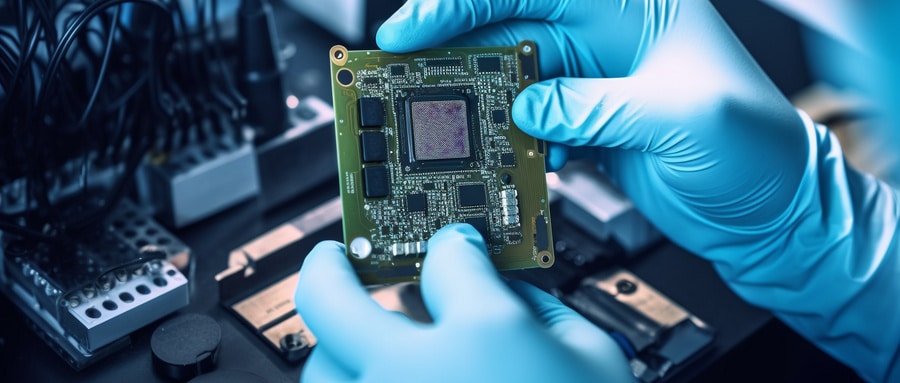
Conclusion: Silkscreen plays an essential role in PCB design. From assembly, testing and troubleshooting of PCBs, silkscreen must be understood thoroughly by everyone involved with designing or assembling PCBs–from engineers to technicians. Although not as conspicuous, its contribution towards efficient circuit board assembly and maintenance cannot be overstated.
FAQ:
- What is silkscreen PCB?
The silkscreen on a Printed Circuit Board (PCB) is the layer of ink traces used to identify components, test points, parts of the circuit, and other information that is useful to an engineer or assembler. It is named silkscreen because the process was originally done with a method similar to silkscreen printing. - What information does a silkscreen pcb typically include?
A silkscreen pcb typically includes component designators, switch settings, test points, polarity marks, warning symbols, company logos, and copyright information. - Which side of the PCB is the silkscreen applied to?
The silkscreen can be applied to either or both sides of the PCB, depending on the design. In most cases, it is applied on the component side to help with assembly. - What materials are used for silkscreen PCB production?
The materials used for silkscreening can vary but are primarily epoxy-based inks. The color is most often white, but other colors like black, yellow, or red are sometimes used for better contrast against the board color. - How is the silkscreen applied in PCB production?
The silkscreen is typically applied using one of two methods: traditional screen-printing technique or inkjet printing. Both methods can produce high-quality results, but inkjet printing offers more flexibility and is faster for high-volume production. - Can the silkscreen wear off?
Silkscreening PCB production is designed to be permanent and should resist standard handling and soldering processes. It should not wear off under normal circumstances. - Are silkscreens on PCBs mandatory?
Silkscreens are not mandatory, but they make silkscreen PCB assembly, troubleshooting, and maintenance considerably easier. Without a silkscreen, engineers and assemblers need to rely on the layout files to understand the board. - Can I include my company logo on the silkscreen pcb?
Yes. Company logos can be added to the silkscreen. However, they need to fit into the designated board space without interfering with the board function or clarity of important information. - Are there standards I should follow for silkscreen nomenclature?
Standards such as IPC-2612, published by the Association Connecting Electronics Industries, provide guidelines for PCB artwork, including silkscreen. Following these industry standards can improve the quality and usability of PCBs. - How is silkscreen quality checked in PCB production?
The silkscreen layer is usually checked during the quality control process. Checks include the clarity of the print, the presence of all intended markings, the correct placement on pads, and the absence of ink smears or misprints.

