Flexible PCB Manufacturing: Exploring the Advantages and Process of Flexible Printed Circuit Boards
Flexible printed circuit boards (PCBs) have revolutionized the electronics industry with their ability to bend, twist, and conform to complex shapes. In this article we’ll delve into flexible PCB manufacturing and explore its many benefits as well as the manufacturing process involved.
Advantages of Flexible PCBs:
- Space Optimization: Flex PCBs are ultra thin and lightweight, making efficient use of space in electronic devices with limited footprint. They can easily fit into tight spots or wrap around other components to free up room for other functions while conserving valuable surface area for other uses.
- Increased Reliability: Flexible PCBs offer increased reliability by eliminating traditional wire harnesses, connectors and solder joints to reduce potential points of failure. Furthermore, mechanical connectors eliminate signal distortion, electromagnetic interference (EMI) issues as well as vibration-related concerns that arise with traditional wiring harnesses and solder joints.
- Improved Flexibility and Durability: Flexible PCBs have long been valued for their superior flexibility and durability, making them suitable for applications where mechanical motion or vibration may be a concern, such as wearable devices, automotive electronics or aerospace systems.
- Cost-Effective Manufacturing: Thanks to advances in manufacturing techniques, flexible PCBs can now be produced at lower costs compared to their rigid counterparts. Consolidating multiple interconnects onto one flexible circuit board enables assembly processes to move more quickly and reduce production efficiency costs simultaneously.
Flexible PCB Manufacturing Process: An Overview
- Design and Material Selection: The initial step in flexible PCB manufacturing involves designing the circuit layout and selecting suitable materials, taking into account factors like desired flexibility, component placement, signal integrity and thermal management. These flexible boards often use polyimide films, copper foils, adhesives and coverlay films.
- Circuit Patterning: Once materials have been chosen, they are coated with a photosensitive layer. After exposure with a high-resolution photomask, an unwanted copper is removed using either chemical etching or laser ablation processes.
- Layer Bonding: At this step, multiple layers of the flexible PCB are laminated together using heat and pressure, using adhesive films or heat-activated glues between them to form an integrated structure.
- Drilling and Plating: Small holes called vias are drilled through a flexible PCB to connect different layers, before being coated with an electrically conducting material like copper plating to ensure continuity in electrical transmission.
- Component Assembly: Two types of assembly technologies used on flexible PCBs for component installation are surface mount technology (SMT) and through-hole technology (THT). SMT components can be directly adhered onto the PCB using solder paste; THT components require inserting leads into predrilled holes before soldering them at their opposite ends.
- Testing and Inspection: Once assembled, flexible PCBs undergo thorough testing and inspection to ensure their functionality and reliability. Various tests such as continuity testing, electrical testing and functional validation can be run to validate its performance.
- Coverlay Application: In order to protect the circuitry on flexible PCBs, a coverlay film must be applied over its surface. A flexible dielectric material called coverlay acts as an insulating layer while providing mechanical stability.
- Routing and Final Inspection: After routing is complete, excess material or unnecessary areas are removed by using routing torches. A final inspection ensures maximum quality before it is shipped off to customers.
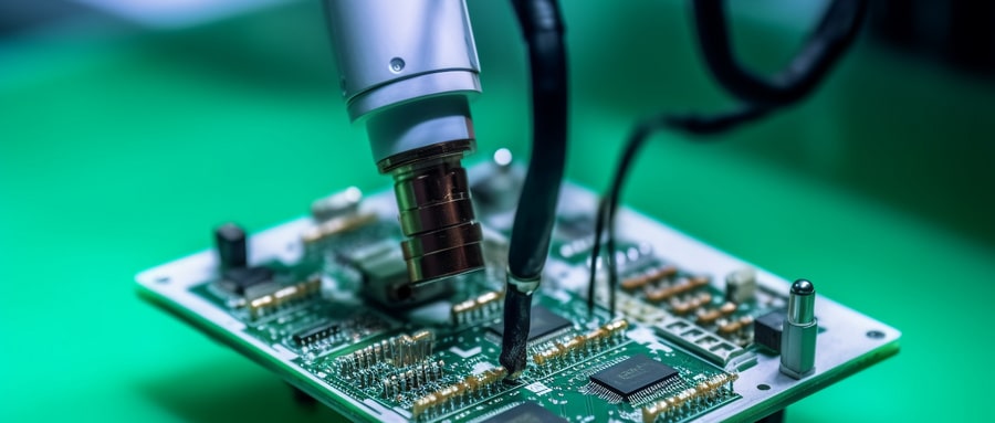
Flexible PCB manufacturing offers numerous advantages, including space optimization, improved reliability, flexibility and cost-effectiveness. The intricate process involved in producing flexible PCBs includes careful design, material selection, layer bonding drilling testing coverlay application routing inspection as well as final inspection. As technology evolves further flexible PCBs will play a vital role in driving innovation in electronic devices across industries.
Flexible PCB Manufacturing FAQ:
- What is Flexible PCB manufacturing?
Flexible PCB manufacturing refers to the process of producing Printed Circuit Boards (PCBs) that are designed to exhibit flexibility. This flexibility allows the board to bend or flex during use, enabling unique configurations and dynamic motion within the device. - What materials are used in Flexible PCB manufacturing?
The most common material used as the base for flexible PCBs is polyimide, a flexible, heat-resistant, and electrically-insulated plastic. Copper is typically used for the conductor layer, and a flexible solder mask is applied as a protective coating. - What is the process of Flexible PCB manufacturing?
The process involves designing the circuit, preparing and cleaning the polyimide and copper combination, etching to remove unnecessary copper, drilling holes if needed, and applying solder mask to protect the circuitry. Components are then attached using surface mount technology. - What are the advantages of Flexible PCBs?
Flexible PCBs are lightweight, can withstand high temperatures, and can be folded without causing damage. They save space and can be conformed to fit into tiny or irregularly shaped spaces. They also reduce the need for wires and connectors, which helps in reducing overall system failure rate. - What are the applications of Flexible PCB manufacturing?
They are often used in devices that have limited space or require a board to be bent at installation or to withstand frequent bending during operation. Applications include smartphones, wearable devices, LCD displays, implantable medical devices, and automotive electronics. - What are the challenges in Flexible PCB manufacturing?
Challenges include controlling the flexibility of the board, handling and aligning the thin and flexible substrates during manufacturing, and ensuring the reliability of the board especially at the folds. - What are Rigid-Flex PCBs?
Rigid-Flex PCBs combine the advantages of both rigid and flexible PCBs. They consist of multiple layers of flexible PCBs sandwiched between rigid PCBs, which are fused together during lamination. - What kind of tools are used for Flexible PCB Design?
CAD (Computer-Aided Design) tools with specific functionality for flex PCBs are used to design these complex circuits. They take into account the board’s curvature, and help predict stress and strain on circuits and solder joints. - What should be considered in the design phase of Flexible PCB?
Among key considerations are the bending radius, the number and location of folds, placement of stiffeners to support components and connectors, and the optimal use of space for component placement. - What is the cost of Flexible PCB manufacturing?
The cost of manufacturing a flexible PCB typically is higher than that of a normal rigid PCB, due to the specialized materials used and the complexity of the manufacturing process. However, this can often be offset by the savings in overall system cost, due to reduction in additional components like connectors and cables.

