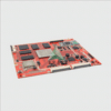
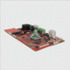
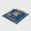
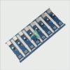
Flash gold pcb, 3 things you know about it?
– Using hard gold plating on PCBs can improve their durability and resistance to wear and tear.
Printed Circuit Boards (PCBs) are essential components in electronic devices. They connect the various electronic components and ensure proper functioning of the device. However, PCBs are prone to wear and tear due to the constant exposure to environmental factors such as humidity, temperature, and mechanical stress. This can lead to corrosion, oxidation, and failure of the PCBs.
One solution to this problem is the use of hard gold plating on PCBs. Hard gold plating is a process where a layer of gold is deposited onto the surface of the PCB using an electroplating technique. This layer of gold is much harder than the traditional soft gold plating, which makes it more durable and resistant to wear and tear.
The hard gold plating process involves the deposition of a thin layer of nickel onto the surface of the PCB, followed by a layer of gold. The nickel layer acts as an intermediate layer between the gold and the PCB substrate, providing better adhesion and preventing peeling or flaking of the gold layer.
The thickness of the gold layer can vary depending on the intended application of the PCB. Typically, a thickness of 5-50 microinches is used for most applications. However, for applications that require higher durability and resistance to wear and tear, a thickness of up to 200 microinches can be used.
Hard gold plating has several advantages over traditional soft gold plating. Firstly, it provides better corrosion and oxidation resistance. This is because the hard gold layer is much less prone to surface contamination and chemical reactions, which can cause corrosion and oxidation.
Secondly, hard gold plating provides better wear resistance. The hard gold layer is much more durable and resistant to mechanical stress, which can cause wear and tear on the PCB. This makes it particularly useful for applications where the PCB is subject to constant mechanical stress, such as in high vibration environments.
Thirdly, hard gold plating provides better electrical conductivity. Gold is an excellent conductor of electricity, and the hard gold layer provides a low resistance path for the flow of electrical current. This can improve the performance of the PCB, particularly in applications where high-speed data transfer is required.
In conclusion, the use of flash gold plating on PCBs can significantly improve their durability and resistance to wear and tear. This makes it a particularly useful solution for applications where the PCB is subject to harsh environments or constant mechanical stress. By improving the reliability and performance of PCBs, hard gold plating can help to ensure the proper functioning of electronic devices and reduce the need for maintenance and repairs.
– Flash gold PCBs can be used in harsh environments, such as aerospace or military applications.
Flash Gold PCB: The Powerhouses of Harsh Environments
Printed Circuit Boards (PCBs) have become an integral part of modern electronic devices. They provide a platform for the components to communicate with each other and function together. However, not all PCBs are created equal. Regular PCBs may not be able to withstand the rigors of harsh environments such as aerospace or military applications. That is where Hard Gold PCBs come into the picture.
Flash Gold PCBs are PCBs that have a coating of hard gold on their surface. The coating is made up of a mixture of gold and other metals such as nickel and cobalt. The thickness of the coating varies depending on the requirements of the application. The gold coating provides several benefits over regular PCBs, making them ideal for harsh environments.
One of the main advantages of Hard Gold PCBs is their exceptional durability. The gold coating is highly resistant to wear and tear, making it ideal for applications where the PCB is subjected to frequent use or exposure to harsh conditions. The coating also protects the PCB from corrosion, which can damage the components and lead to malfunction.
Another significant advantage of Hard Gold PCBs is their ability to withstand high temperatures. The gold coating has a high melting point, making it ideal for applications where the PCB is exposed to high temperatures, such as in aerospace or military applications. The coating also has excellent electrical conductivity, making it ideal for applications where the PCB is required to transmit high currents.
Flash Gold PCB are also highly reliable. The gold coating provides a stable and consistent surface for the components to be mounted on, ensuring that they are securely held in place and do not come loose due to vibration or shock. The coating also provides a reliable connection between the components and the PCB, ensuring that the signals are transmitted accurately and without interference.
In conclusion, Flash Gold PCBs are an excellent choice for applications that require durability, high-temperature resistance, and reliability. They are commonly used in aerospace, military, and medical applications, where the PCBs are subjected to harsh conditions. The gold coating provides an extra layer of protection and ensures that the PCB performs optimally, even in the harshest of environments.

