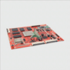
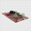
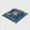
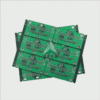
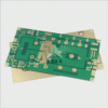
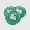
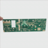
6 layers PCB boards are more widely used?
A 6 layers pcb consists of six layers of conductive material. It consists of two planes between a 4 layers pcb and two additional signal layers. A typical 6 layers printed circuit board consists of two inner layers, two outer layers and two inner layers, one for power and one for ground. This design improves EMI and provides better routing for low and high speed signals. A 2 layers surface layer helps in the transmission of low-speed signals, while the two inner layers help in high-speed signals.
6 Layers PCB
Correctly stacking a 6 layers PCB can lead to perfect performance, it can effectively suppress EMI due to the use of different kinds of RF devices and contains multiple spacing components. Any error in the design will affect the perfect performance of the PCB. So how should we design to fully utilize the perfect performance of PCB?
First of all before designing, we need to analyze and address the number of ground, power and signal planes that the pcb may need. Grounding planes are an important part of any laminate because they provide better shielding for the laminate and they reduce the need for external shielding cans.
If you want to plan dense boards where wiring takes up little space, you can install four signal planes, one ground plane and one power plane. In denser boards, where a mix of wireless and analog signals is used, the signal/ground/power/ground/signal/ground layers are stacked in such a way as to separate the internal and external signal layers, and there are both internal and external signal layers. This layered design helps to suppress the internal signal layer EMI mixing. The stacked design is also ideal for RF equipment because the AC power and ground layers provide excellent decoupling.
Dense Circuit Boards
If you want to build a printed circuit board with a lot of sensitive traces, it is best to choose a stack like this: Signal/Power/2Signal/Ground/Signal. This provides excellent protection for sensitive traces and is better suited for circuits that employ high-frequency analog signals or high-speed digital signals. These signals will be separated from the lower speed signals in the outer layer. This shielding is accomplished in the inner layer, which also allows signals of different frequencies or switching speeds to be routed.
Printed Circuit Board
Ground/Signal Layer/Power/Ground/Signal Layer/Ground stacking can be perfectly deployed for circuit boards in the vicinity of strong radiation sources. This stacking effectively suppresses electromagnetic interference and is also suitable for boards used in noisy environments.
Since their 6 layers pcb design has become a common feature of some advanced electronic circuits popular among electronics manufacturers, what are its specific advantages?
6 Layers PCB Design
Due to their multilayer design, they are relatively smaller than other circuit boards, which is especially beneficial for micro devices.The design of a 6 layers PCB stack requires a great deal of planning, which reduces errors in detail and ensures high quality construction. Different testing and inspection techniques are now generally used to ensure the suitability of the boards.
Compact printed circuit boards are achieved by using lightweight components, which helps to reduce the overall weight of the printed circuit board. Unlike single or double layer PCB, 6 layers PCB can interconnect components without multiple connectors.
A 6 layers PCB consists of multiple insulating layers that are made of protective materials bonded to different prepregs. This contributes to the durability of these PCB.
With excellent electrical performance and compact design, 6 layers PCB are effective in ensuring high speed and high capacity.

